This blog post is part of a series called “CommScope Definitions” in which we will explain common terms in communications network infrastructure.
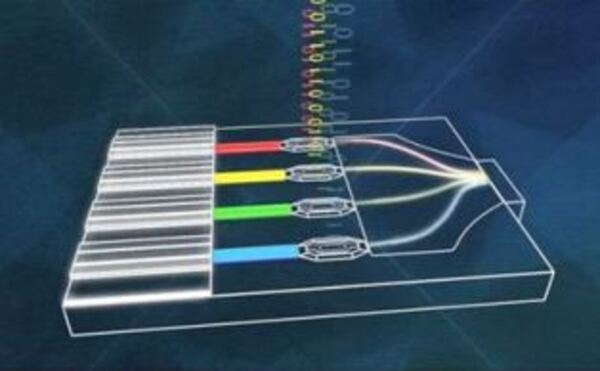
Silicon photonics (SiPh) is a technology that involves data being transferred among computer chips by optical rays. On the surface, it seems simple, but it can actually be difficult to understand. Perhaps it is best to compare it to an electrical circuit.
In the early days of electrical circuits, there were discrete components (e.g., transistors, capacitors, resistors, etc.) that were connected with traces on a printed circuit board. In order to reduce size and cost, many discrete components were formed adjacently and interconnected on a single silicon substrate to create integrated circuits (i.e. chips). Over time, the types of components that could be formed on chips continued to expand while their size and power consumption shrank at dramatic rates (per Moore’s law). We now have billions of interconnected components per chip, each at a negligible cost.
The objective of silicon photonics is to enable the same cost effective component integration in the optical domain. Specifically, optical components (e.g. lasers, splitters, modulators, combiners, etc) are interconnected with transparent pathways or waveguides for light to travel through, much like electricity runs through traces on a circuit board. The industry has focused on leveraging the investments made in silicon by the electrical chip industry wherever possible.
SEE ALSO: Silicon photonics market to grow 21% from 2016 to 2022
Although the technical capability of SiPh has continually progressed, two related challenges have kept the cost of SiPh solutions high:
- It is not possible to form lasers directly in silicon. Instead, lasers are made out of other materials, and their output (light) is coupled into the waveguides.
- SiPh waveguides are small, making interconnections to and from the chips difficult and expensive. Specifically, SiPh waveguides are less than half a micron in diameter which is about 1/20th the diameter of today’s standard single mode fiber. Various alignment techniques are available, but they are expensive.
An approach that is having significant market impact is to replace the pure silicon substrate with silicon dioxide (i.e., glass). The resulting circuit is called Photonic Light Circuit (PLC). The types of components that can be formed on PLCs is limited, but the use of glass substrates allows six times larger waveguides which reduces the alignment challenges to other components like lasers. The combination of technologies is helping solve challenges and driving down the cost of high speed photonics. It also redefines the industry’s direction from purely “silicon photonics” to the wider field of “integrated photonics.” CommScope tracks these developments closely as they impact the optimal choice of fiber type in multiple markets we serve.
Are you seeing intriguing developments around integrated photonics? Comment here, and we’ll have a discussion that will keep all of us up to date with architectural advancements in this exciting field.


